- 您现在的位置:买卖IC网 > Sheet目录2006 > LTC2451ITS8#TRPBF (Linear Technology)IC ADC 16BIT DELTA SIG TSOT23-8
LTC2451
15
2451fg
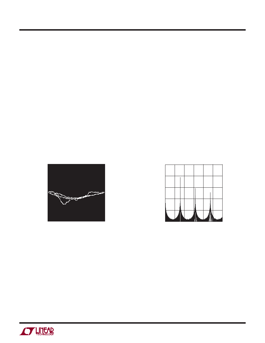
Figure 13. Measured INL vs Input Voltage,
CIN = 0, VCC = 5V, TA = 25°C
Figure 14. LTC2451 Input Signal Attenuation vs Frequency
either in sleep or I/O modes. Thus, if the time constant of
the input RC circuit
t = RS CIN, is of the same order of
magnitude or longer than the time periods between actual
conversions, then one can consider the input current to
be reduced correspondingly.
These considerations need to be balanced out by the input
signal bandwidth. The 3dB bandwidth ≈ 1/(2
pRSCIN).
Finally, if the recommended choice for CIN is unac-
ceptable for the user’s specific application, an alternate
strategy is to eliminate CIN and minimize CPAR and RS.
In practical terms, this configuration corresponds to a
low impedance sensor directly connected to the ADC
through minimum length traces. Actual applications
include current measurements through low value sense
resistors, temperature measurements, low impedance
voltage source monitoring, and so on. The resultant INL
versus VIN is shown in Figure 13. The measurements of
Figure 13 include a capacitor CPAR corresponding to a
minimum sized layout pad and a minimum width input
trace of about 1" length.
Signal Bandwidth and Noise Equivalent Input
Bandwidth
TheLTC2451includesasinc1typedigitalfilterwiththefirst
notch located at f0 = 60Hz. As such, the 3dB input signal
bandwidthis26.54Hz.ThecalculatedLTC2451inputsignal
attenuation versus frequency over a wide frequency range
is shown in Figure 14. The calculated LTC2451 input signal
attenuation with low frequencies is shown in Figure 15.
The converter noise level is about 1.4VRMS, and can be
modeled by a white noise source connected at the input
of a noise-free converter.
APPLICATIONS INFORMATION
INPUT
SIGNAL
A
TTENUA
TION
(dB)
–40
0
2451 F14
–60
–80
–20
–100
INPUT SIGNAL FREQUENCY (MHz)
0
1.00
1.25
1.50
2.5
5.0
7.5
INPUT VOLTAGE (V)
0
INL
(LSB)
8
6
4
2
0
–2
–4
–6
–8
4
2451 F13
1
2
3
5
3.5
0.5
1.5
2.5
4.5
RS = 1k
RS = 10k
RS = 0
发布紧急采购,3分钟左右您将得到回复。
相关PDF资料
LTC2452ITS8#TRPBF
IC ADC 16BIT DELTA SIG TSOT23-8
LTC2453ITS8#TRMPBF
IC ADC 16BIT DELTA SIG TSOT23-8
LTC2482IDD#TRPBF
IC ADC 16BIT 10-DFN
LTC2483IDD#TRPBF
IC ADC 16BIT I2C 10-DFN
LTC2485CDD#TRPBF
IC ADC 24BIT I2C 10-DFN
LTC2487CDE#PBF
IC ADC 16BIT DELTA SIG 14-DFN
LTC2492IDE#TRPBF
IC ADC 24BIT DELTA SIG 14-DFN
LTC2493IDE#TRPBF
IC ADC 24BIT DELTA SIG 14-DFN
相关代理商/技术参数
LTC2452CDDB#PBF
制造商:Linear Technology 功能描述:ADC Single Delta-Sigma 60sps 16-bit Serial 8-Pin DFN EP 制造商:Linear Technology 功能描述:Bulk
LTC2452CDDB#TRMPBF
功能描述:IC ADC 16BIT DELTA SIG 8-DFN RoHS:是 类别:集成电路 (IC) >> 数据采集 - 模数转换器 系列:- 产品培训模块:Lead (SnPb) Finish for COTS
Obsolescence Mitigation Program 标准包装:1 系列:- 位数:10 采样率(每秒):357k 数据接口:DSP,MICROWIRE?,QSPI?,串行,SPI? 转换器数目:1 功率耗散(最大):830µW 电压电源:单电源 工作温度:-40°C ~ 85°C 安装类型:表面贴装 封装/外壳:10-WFDFN 裸露焊盘 供应商设备封装:10-TDFN-EP(3x3) 包装:剪切带 (CT) 输入数目和类型:2 个单端,单极;2 个单端,双极;1 个差分,单极;1 个差分,双极 产品目录页面:1396 (CN2011-ZH PDF) 其它名称:MAX1395ETB+TCT
LTC2452CDDB#TRPBF
功能描述:IC ADC 16BIT DELTA SIG 8-DFN RoHS:是 类别:集成电路 (IC) >> 数据采集 - 模数转换器 系列:- 标准包装:2,500 系列:- 位数:16 采样率(每秒):15 数据接口:MICROWIRE?,串行,SPI? 转换器数目:1 功率耗散(最大):480µW 电压电源:单电源 工作温度:-40°C ~ 85°C 安装类型:表面贴装 封装/外壳:38-WFQFN 裸露焊盘 供应商设备封装:38-QFN(5x7) 包装:带卷 (TR) 输入数目和类型:16 个单端,双极;8 个差分,双极 配用:DC1011A-C-ND - BOARD DELTA SIGMA ADC LTC2494
LTC2452CTS8#PBF
制造商:Linear Technology 功能描述:Bulk 制造商:Linear Technology 功能描述:MS-ADC/Delta Sigma, CUT TAPE 16-bit 60Hz SPI Different Ultra-Tiny Delta Sigma ADC
LTC2452CTS8#TRMPBF
功能描述:IC ADC 16BIT DELTA SIG TSOT23-8 RoHS:是 类别:集成电路 (IC) >> 数据采集 - 模数转换器 系列:- 标准包装:1 系列:microPOWER™ 位数:8 采样率(每秒):1M 数据接口:串行,SPI? 转换器数目:1 功率耗散(最大):- 电压电源:模拟和数字 工作温度:-40°C ~ 125°C 安装类型:表面贴装 封装/外壳:24-VFQFN 裸露焊盘 供应商设备封装:24-VQFN 裸露焊盘(4x4) 包装:Digi-Reel® 输入数目和类型:8 个单端,单极 产品目录页面:892 (CN2011-ZH PDF) 其它名称:296-25851-6
LTC2452CTS8#TRPBF
功能描述:IC ADC 16BIT DELTA SIG TSOT23-8 RoHS:是 类别:集成电路 (IC) >> 数据采集 - 模数转换器 系列:- 标准包装:2,500 系列:- 位数:16 采样率(每秒):15 数据接口:MICROWIRE?,串行,SPI? 转换器数目:1 功率耗散(最大):480µW 电压电源:单电源 工作温度:-40°C ~ 85°C 安装类型:表面贴装 封装/外壳:38-WFQFN 裸露焊盘 供应商设备封装:38-QFN(5x7) 包装:带卷 (TR) 输入数目和类型:16 个单端,双极;8 个差分,双极 配用:DC1011A-C-ND - BOARD DELTA SIGMA ADC LTC2494
LTC2452IDDB#PBF
制造商:Linear Technology 功能描述:ADC Single Delta-Sigma 60sps 16-bit Serial 8-Pin DFN EP 制造商:Linear Technology 功能描述:Bulk
LTC2452IDDB#TRMPBF
功能描述:IC ADC 16BIT DELTA SIG 8-DFN RoHS:是 类别:集成电路 (IC) >> 数据采集 - 模数转换器 系列:- 产品培训模块:Lead (SnPb) Finish for COTS
Obsolescence Mitigation Program 标准包装:1 系列:- 位数:10 采样率(每秒):357k 数据接口:DSP,MICROWIRE?,QSPI?,串行,SPI? 转换器数目:1 功率耗散(最大):830µW 电压电源:单电源 工作温度:-40°C ~ 85°C 安装类型:表面贴装 封装/外壳:10-WFDFN 裸露焊盘 供应商设备封装:10-TDFN-EP(3x3) 包装:剪切带 (CT) 输入数目和类型:2 个单端,单极;2 个单端,双极;1 个差分,单极;1 个差分,双极 产品目录页面:1396 (CN2011-ZH PDF) 其它名称:MAX1395ETB+TCT